Early tests of a domestic deep‑ultraviolet scanner point to a path around U.S. export curbs — but yields and timelines remain the biggest hurdles

China’s top chipmaker Semiconductor Manufacturing International Corp (SMIC) has begun running limited production trials on the country’s first domestically built advanced deep‑ultraviolet (DUV) lithography machine, according to multiple people familiar with the effort. The early testing marks a pivotal moment in Beijing’s campaign to insulate its semiconductor supply chain from Western export controls and to close the gap with global leaders.
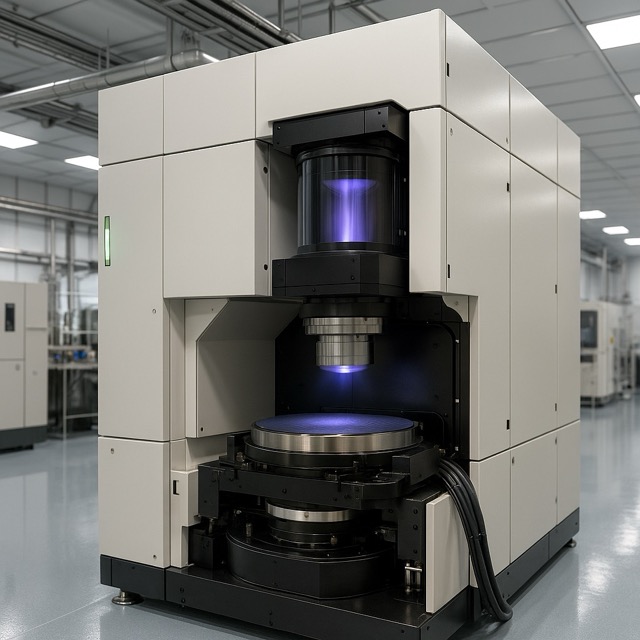
The tool under evaluation is an argon‑fluoride (ArF) immersion‑class DUV scanner made by Shanghai‑based start‑up Yuliangsheng, whose backers include the industrial platform SiCarrier. While far short of the extreme‑ultraviolet (EUV) systems that enable the most advanced chips elsewhere, a reliable domestic ArF immersion platform would allow Chinese fabs to push beyond 28‑nanometre production using multi‑patterning techniques—potentially supporting 7nm‑class system‑on‑chips for smartphones and AI accelerators at modest yields.
Two people with knowledge of the trials said the machine has been run in short, closely supervised stints on a 300‑millimetre line, with initial process windows focused on overlay stability, critical dimension uniformity and defectivity. Engineers cautioned that qualification for round‑the‑clock production typically takes at least a year on any new lithography platform and longer when the supply chain is still being localized.
The stakes are high. The Netherlands has restricted shipments of ASML’s most capable DUV immersion tools to China since early 2024, and U.S. rules issued late last year expanded controls on a broad range of chip‑equipment categories. Unable to buy or service top‑end scanners at will, Chinese manufacturers have poured resources into domestic alternatives. If SMIC can stabilize yields with home‑grown DUV equipment, it would blunt the bite of those measures—even if EUV remains off‑limits.
People briefed on the project said most major sub‑modules in the Yuliangsheng system are sourced in China, including the wafer stage, computational lithography software, and parts of the projection optics. Some specialty components—such as laser subsystems, ultra‑high‑purity materials and certain metrology sensors—still depend on imports that face their own licensing uncertainties. Securing redundant suppliers for those choke‑points is a priority of the trial program.
Any ramp will hinge on yield. At 28nm single‑patterning, fabs expect relatively forgiving defect density and overlay budgets. But when the same DUV platform is stretched to 14nm, 10nm or 7nm through double, triple or even quadruple patterning, the process margin collapses. That demands exceptionally tight stage control, resist chemistry and etch fidelity across many more steps—where compounding errors can devastate wafer output.
Even partial success would matter. China’s handset and cloud vendors have already shown a willingness to design around constraints, accepting die‑size and power trade‑offs to keep supply chains domestic. For AI inference, for example, clusters of mid‑range accelerator chips can substitute for a smaller number of cutting‑edge processors—provided total cost of ownership, electricity and software efficiency remain competitive.
Market reaction has been swift. Shares of SMIC and several China‑listed equipment names rose in Wednesday trading after reports of the trials circulated, reflecting hopes that qualification could begin to ease dependence on restricted foreign tools. Analysts cautioned, however, that commercialization milestones should be measured in quarters and years, not weeks.
Inside the cleanroom, engineers are chasing three early milestones. First is overlay repeatability on product wafers under full‑flow conditions, not just test exposures. Second is uptime—can the tool run stably for consecutive days without service interventions that break the line? Third is matching: even if one machine works, a fab needs multiple tools to match exposure signatures so lots can move between bays without yield penalties.
Beyond lithography, localization of the broader patterning stack is accelerating. Domestic suppliers in etch, deposition, cleaning and photoresist have added 300mm‑class tools and materials over the past two years, though availability at the leading edge remains uneven. Industry managers describe a pragmatic approach: deploy homegrown subsystems where risk is manageable, mix in imported pieces where necessary, and advance stepwise rather than attempting a single ‘Big Bang’ conversion.
Yuliangsheng’s emergence adds complexity to an already crowded field. Shanghai Micro Electronics Equipment (SMEE) announced a 28nm‑capable immersion platform in late 2023, but it has not provided public shipment details for high‑volume manufacturing. Whether China consolidates around one domestic architecture or pursues several in parallel will influence tooling compatibility, service models and the pace of software ecosystem development.
For Washington and its allies, the trials underscore the limits—as well as the effectiveness—of export controls. Restrictions have undeniably slowed China’s access to the most advanced manufacturing gear and raised costs. Yet they have also incentivized redundant domestic programs that, over time, can close portions of the gap. Policymakers face a moving target: each tightening buys time but encourages substitutions across the value chain.
Industry veterans note that DUV immersion is a known quantity. The physics are hard, but they are tractable—especially with high‑NA EUV now absorbing the frontier R&D burden in other markets. The real challenge is execution: tuning vibration isolation, perfecting optical coatings, writing robust control firmware and building a field‑service organization capable of supporting dozens of tools across multiple fabs.
A key unknown is computational lithography. Multiple‑patterning flows at advanced nodes lean heavily on sophisticated OPC (optical proximity correction), inverse lithography and model‑based process control. China has strong algorithm talent and growing EDA start‑ups, but tight integration between scanner telemetry and fab‑wide APC (advanced process control) loops takes time to mature—especially when some libraries and models remain export‑controlled.
People close to SMIC say internal roadmaps envision a staged rollout: use domestic DUV for mature‑node capacity additions first, qualify a small number of critical layers on more advanced nodes next, and only then attempt full flows. In parallel, procurement teams are pursuing licenses for select foreign sub‑modules to de‑risk bottlenecks. No timeline has been set publicly, and engineers stress that yield—not the calendar—will decide go‑live dates.
If successful, the payoff is strategic. A credible ArF immersion stack would let Chinese foundries expand production of 14/12nm, 10nm and 7nm‑class chips without relying on new imports of restricted tools. That would support a wider domestic ecosystem—from smartphones and routers to data‑center AI—while leaving the EUV threshold for 5nm and beyond as a separate, longer‑term challenge.
Skeptics counter that even perfecting DUV is not enough. Advanced memory still leans on process modules and materials dominated by foreign suppliers. Packaging at the cutting edge requires high‑density substrates, hybrid bonding and through‑silicon‑via steps where domestic capability is uneven. And software—the compilers, graph libraries and AI frameworks that make chips useful—remains an underappreciated constraint on system performance.
For now, SMIC’s trial is a test of persistence. It will demand thousands of small engineering wins: a fraction of a nanometre shaved from overlay here, a percentage point of uptime there, a material impurity knocked down by another nine. Each improvement compounds. Whether that adds up to a production‑worthy platform in the next 12–18 months will be the most closely‑watched question in China’s technology policy.
What is clear is that the center of gravity is shifting. China’s equipment champions—established players and ambitious start‑ups alike—are no longer chasing only lab demos. They are installing hardware on real lines, on real wafers, under the harsh light of factory KPIs. That is the point where engineering resolves into economics. And if the numbers work, the politics will follow.