Multi‑year contract—reportedly with Tesla—extends through 2033, bolstering Samsung’s U.S. footprint as AI-era demand reshapes the semiconductor market

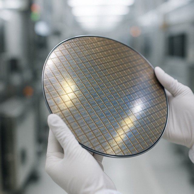
SEOUL / AUSTIN — Samsung Electronics has signed a KRW22.8 trillion (~$16.5 billion) contract to supply semiconductors to a major global customer, a milestone that signals the South Korean giant’s most assertive push yet to win back share in advanced manufacturing and to cement its role in the surging AI supply chain. While neither party officially disclosed the buyer, multiple industry reports indicate the agreement is tied to Tesla’s next‑generation AI6 system‑on‑chip to be produced at Samsung’s Taylor, Texas facility. The deal runs through the end of 2033, underscoring how long‑dated chip programs are becoming in the AI and automotive era.
The announcement lands at a pivotal moment for Samsung. After a bruising downturn in 2023 and an intense 2024–25 scramble for high‑bandwidth memory (HBM) capacity, Samsung is regaining momentum as conventional memory prices rebound and as foundry customers look to dual‑source beyond Taiwan Semiconductor Manufacturing Company (TSMC). For Texas, the contract represents one of the clearest anchors yet for Samsung’s multibillion‑dollar U.S. bet, spanning advanced logic, packaging, and a broader local ecosystem of materials and equipment suppliers.
Strategically, the contract could be more consequential than its headline value suggests. Automotive and robotics workloads increasingly resemble data‑center AI in their appetite for compute per watt, and carmakers are converging on custom silicon to control cost, roadmap cadence, and supply security. If Tesla’s AI6 program successfully ramps at Taylor, it will validate Samsung’s EUV process maturity in the United States and could unlock follow‑on work across automotive, edge AI, and even hyperscale accelerators.
Equally important is the signal this sends across the geopolitical chessboard. Washington’s push to localize critical nodes—fabs, advanced packaging, and trusted supply—has pushed chip makers to thread a needle: stay close to leading customers while mitigating tariff and export‑control risk. By anchoring a marquee AI processor program in Texas, Samsung not only aligns with U.S. policy incentives but also reduces logistics complexity for North American customers integrating chips into vehicles and data‑center hardware.
In the near term, execution risk looms largest. Samsung has spent the past two years closing perceived gaps with rivals in HBM reliability and in leading‑edge logic yield. Ramping a complex, high‑power automotive‑grade SoC at competitive performance, cost, and yield will test those improvements. Foundry veterans note that automotive silicon layers in additional qualifications—functional safety (ISO 26262), extended temperature ranges, and long service lifetimes—that can stretch schedules if early silicon requires spins. The 2025–2026 window will be the first proving ground for Taylor’s sustained high‑volume performance on those metrics.
The timing also intersects with a sharp turn in memory cycles. As AI servers absorb unprecedented volumes of DRAM and NAND, spot and contract prices have rebounded, improving Samsung’s profitability and cash generation. That matters for a capital‑intensive foundry ramp: EUV tools, power and water infrastructure, and clean‑room expansions all compete for budget against HBM capacity additions. Investors have rewarded the prospect of balanced growth—memory pricing tailwinds funding a renewed foundry push—yet will watch gross margin cadence closely as the Taylor site moves from pre‑production to scale.
For Tesla, the calculus is similarly strategic. Custom compute remains core to the company’s autonomy roadmap, training clusters, and a growing interest in humanoid robotics. A secure multi‑year wafer and packaging allocation from a U.S. site offers tighter control over product refreshes and mitigates transport risk for sensitive, high‑value silicon. If program milestones are met, the arrangement could also broaden into advanced packaging—2.5D and 3D integration—where proximity to U.S. OSAT partners shortens cycle times for chiplet architectures trending across the industry.
The broader foundry market will read the deal through the lens of competition with TSMC and the resurgence of GlobalFoundries and Intel Foundry Services in the United States. Samsung’s differentiator has long been its ability to swing capacity between memory and logic; the challenge is converting that flexibility into best‑in‑class yields at the most advanced nodes. With automotive and edge AI favoring power efficiency and cost over absolute bleeding‑edge density, Samsung has an opening to accumulate reference wins and rebuild mindshare with system companies that once defaulted to TSMC.
Policy dynamics remain a wild card. New tariff proposals on chip‑dense imports, evolving export controls on equipment and materials, and the pace of CHIPS Act disbursements can all tip the economics of U.S. production. Supply chain leaders say the shift toward ‘local‑for‑local’ production will persist regardless, but incentive timing affects when capacity comes online—and which products get priority for U.S. ramps.
Looking to 2026–2028, three milestones will determine whether the $16.5 billion contract becomes a beachhead for Samsung’s U.S. foundry franchise: (1) sustained yields and on‑time tape‑outs at Taylor across at least two process generations; (2) visible expansion of advanced packaging alongside logic, enabling chiplet‑based designs at scale; and (3) a diversified customer mix beyond the anchor program, spreading fixed costs and smoothing utilization. Clear progress on those fronts would position Samsung to contest a larger slice of automotive, AI accelerator, and edge inference silicon in North America.
For now, the contract underscores a market in flux. As AI workloads swell and carmakers morph into compute companies, long‑horizon chip deals are becoming the rule rather than the exception. Samsung’s latest win reflects that structural shift—and sets a high‑stakes to‑do list for the next eight years.
By the numbers
Key Facts:
• Contract value: ~$16.5 billion (KRW22.8 trillion)
• Duration: Orders from July 2025 through Dec. 31, 2033
• Likely customer: Tesla (AI6 program), per multiple reports
• Primary site: Taylor, Texas (logic; potential advanced packaging)
• Strategic context: AI demand, automotive compute, U.S. localization
Reporting: October 2025. Sources include company disclosures and contemporaneous media reports.