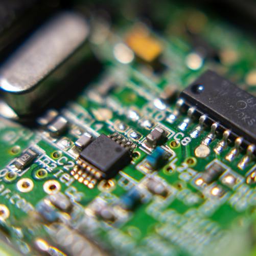
China’s leading DRAM maker says its fifth-generation manufacturing platform has entered mass production, pairing denser process technology with new 24-gigabit LPDDR5X products as export controls and AI demand reshape the global memory-chip contest.

China’s memory-chip ambitions moved from laboratory-scale progress to a more consequential manufacturing test on Sunday, when ChangXin Memory Technologies, better known as CXMT, said its fifth-generation DRAM process platform had entered mass production. Announced at the 2026 World Manufacturing Convention in Hefei, the G5 platform is designed to increase memory density, reduce cost per bit and improve power efficiency while supporting new 24-gigabit LPDDR5X products for smartphones and portable electronics. The company says the platform reaches an active-area half-pitch of 11.95 nanometres, uses self-aligned quadruple patterning, raises capacitor aspect ratio to 45:1 and increases gross dies per wafer by at least 50% compared with its previous platform. Those are significant claims, but the commercial importance will depend on variables the announcement did not disclose, including sustained yield, defect rates, customer qualification and production scale.
A manufacturing milestone, not just a product launch
The announcement matters because memory technology is judged less by a one-off demonstration than by the ability to reproduce billions of microscopic structures economically across large volumes of silicon. DRAM is the working memory inside smartphones, personal computers, servers and many embedded systems. Unlike processors, which execute instructions, DRAM is optimized to hold data temporarily and feed it to computing engines at high speed. Each generation is therefore a manufacturing contest in density, power consumption, speed, reliability and cost per stored bit. A design that looks competitive on paper can still fail commercially if too many dies on each wafer are defective or if the production flow is too expensive to run at scale.
CXMT’s language is deliberately ambitious. In its September 20 statement, the Hefei-based company said the G5 platform’s process capability is closing the gap with the most advanced volume-production memory platforms. Reuters described the development as a claimed breakthrough that could strengthen China’s challenge to Samsung Electronics, SK hynix and Micron Technology, the three companies that have long dominated the global DRAM business. The distinction between a claim and an independently established industry ranking is important. CXMT has published physical process metrics and confirmed mass production, but it has not released the kind of yield curves, defect-density data, wafer-start volumes or independent customer validation that would allow outsiders to make a complete like-for-like comparison with the leaders.
What 11.95 nanometres actually means
The headline technical figure is an active-area half-pitch of 11.95 nanometres in the memory array. In DRAM manufacturing, pitch is one way of describing how tightly repeating features are placed. Smaller spacing generally allows more memory cells to fit into the same area, improving density and increasing the number of potentially saleable chips that can be cut from a wafer. The figure does not mean every feature on the chip is exactly 11.95 nanometres wide, nor should it be read as directly equivalent to the marketing node labels used by logic foundries. Memory and logic processes optimize different structures, and modern node names are not literal measurements of a single transistor dimension.
CXMT says it reached the 11.95-nanometre half-pitch through self-aligned quadruple patterning, or SAQP. Multiple patterning is a way of creating features that are finer than a single lithography exposure can define reliably. Instead of printing the final dense pattern in one step, engineers build it through a sequence of deposition, spacer formation, etching and pattern-transfer stages. Quadruple patterning can effectively multiply pattern density, but it also adds process complexity. Every additional step introduces opportunities for overlay error, line-edge variation, contamination and cost. Achieving tight dimensions is therefore only part of the challenge; controlling those dimensions consistently over an entire 300-millimetre wafer and across thousands of wafers is what determines manufacturability.
The capacitor problem at the heart of DRAM scaling
DRAM stores information using a tiny capacitor paired with an access transistor. As cells shrink laterally, the capacitor still needs to hold enough electrical charge for the memory state to be sensed reliably. That tension has pushed manufacturers toward increasingly tall and narrow capacitor structures. CXMT says the G5 platform reaches an array-capacitor aspect ratio of 45:1, meaning the structure is many times taller than it is wide. Such geometry is difficult to manufacture because deep, narrow features must be etched and coated uniformly without collapsing, pinching off or developing unacceptable variation from the top to the bottom.
The company attributes that result to process-flow redesign and new material integration. It also says the platform uses a DRAM-optimized high-k metal-gate process and reduces the height of the core functional region to 6,762 nanometres. High-k materials are used in semiconductor devices because they can provide strong electrical control while limiting leakage that would otherwise rise as insulating layers become extremely thin. For a memory manufacturer, the point is not simply to build smaller structures but to preserve the electrical margins required for retention, sensing and endurance across temperature and voltage ranges expected in consumer devices.
Why gross dies per wafer could matter more than the node label
CXMT’s most commercially relevant claim may be that G5 can produce at least 50% more gross dies per wafer than its fourth-generation platform when normalized to an 8-gigabit-density baseline. More dies per wafer can lower manufacturing cost per chip because the fixed cost of processing a wafer is spread across a larger number of potential products. That is one of the fundamental economic rewards of semiconductor scaling. It can also allow a producer to expand bit output without increasing wafer starts by the same proportion, an especially valuable advantage when fabrication capacity, equipment availability or power and water infrastructure constrain expansion.
But “gross dies per wafer” is not the same as good dies per wafer. Reuters specifically noted that the metric describes the theoretical or physical number of chips available before defective units are excluded. The missing variable is yield: the percentage of fabricated dies that meet specifications strongly enough to be sold. A 50% increase in gross die count can be transformative if yield remains high, but far less valuable if the denser process suffers a large rise in defects. CXMT’s September 20 release does not disclose production yield, defect density, monthly wafer output or how quickly yield has improved since pilot production. Those numbers will be essential in judging whether G5 changes the economics of the market rather than merely the geometry of the chip.
Two 24-gigabit LPDDR5X products move with the process
Alongside the manufacturing platform, CXMT introduced two LPDDR5X products based on G5. Each has a 24-gigabit capacity per die, which is 50% higher than the company’s previous comparable 16-gigabit products. Since eight bits equal one byte, a 24-gigabit die represents 3 gigabytes of raw storage capacity before multiple dies are combined in a package. Higher per-die capacity allows device makers to reach common smartphone memory configurations with fewer dies, potentially simplifying packaging, reducing board space and lowering power associated with interconnections, although the final benefit depends on the complete product design.
CXMT says the two products use 496-ball and 245-ball package formats and are intended for mid- to high-end smartphones and other portable consumer electronics. Both are already in mass production, according to the company. LPDDR5X is designed for lower-power operation than conventional desktop or server DRAM because battery life and thermal limits are central to mobile devices. Higher density is increasingly important as premium smartphones handle more on-device artificial intelligence, computational photography, gaming and multitasking, all of which create pressure for greater memory capacity and bandwidth without proportional increases in energy use.
Why a new Chinese source of advanced memory is strategically important
The strategic significance extends beyond the specifications of a smartphone memory chip. The modern electronics economy depends on a remarkably concentrated memory supply chain. Samsung, SK hynix and Micron remain the central global suppliers of DRAM, and their capital-investment decisions influence pricing and availability across phones, PCs, data centers, automobiles and industrial electronics. A credible fourth supplier with substantial scale can change procurement behavior even before it matches the leaders in every segment. Customers value second sourcing because memory shortages can halt production of much more expensive finished products.
For China, the issue is sharper. Beijing has spent years trying to reduce dependence on foreign semiconductor technologies, particularly in areas considered essential to computing, communications and national industrial resilience. Memory is not a peripheral component in that strategy. Advanced processors are ineffective without fast memory, while smartphones, servers and artificial-intelligence systems require increasingly large pools of DRAM. A domestic supplier able to make competitive mobile memory at scale can reduce exposure to foreign supply disruptions and give Chinese electronics manufacturers greater bargaining leverage in a market historically shaped by a small number of non-Chinese producers.
Export controls shaped the route to this point
The G5 announcement also lands against the backdrop of U.S. semiconductor export controls that began tightening materially in October 2022 and were strengthened through subsequent rules. The U.S. Commerce Department’s Bureau of Industry and Security has restricted access to categories of advanced computing chips, semiconductor-manufacturing equipment, software and related technology when it judges those items could support China’s advanced-node production or military modernization. In December 2024, BIS added controls covering 24 categories of semiconductor-manufacturing equipment, three categories of software tools and certain high-bandwidth memory, while also expanding the Entity List.
Those controls do not mean that Chinese manufacturers are unable to advance. Instead, they reshape the engineering problem. Companies may need to extend the life of older lithography platforms, use more patterning steps, qualify domestic equipment, redesign processes around available tools and invest more heavily in local materials, metrology and software. CXMT says its G5 platform was developed through computer simulation and joint work with Chinese equipment makers on critical production steps. Its announcement therefore has significance as a process-integration story: the question is not merely whether one company can build a dense memory cell, but whether a broader domestic manufacturing ecosystem can support repeatable production.
A digital twin enters the fab
One of the less visible elements of CXMT’s release is its description of a digital-twin platform spanning design, tape-out, manufacturing and yield maintenance. In semiconductor production, a digital twin can refer to a detailed computational representation of equipment behavior, process steps, materials interactions and statistical variation. The aim is to model how changes in one part of the flow affect downstream results before engineers commit expensive wafers and tool time. CXMT says its virtual research-and-development line incorporates advanced DRAM process models to accelerate development.
That approach reflects a wider shift in chipmaking. As physical dimensions become smaller and process sequences become longer, experimentation in the fab becomes extraordinarily expensive. Simulation can narrow the set of process conditions that need to be tested physically, while manufacturing data can feed back into models to improve control. None of this removes the need for real wafers: materials can behave unexpectedly, equipment drifts, and models are only as good as the data and physics they contain. But in a constrained equipment environment, the ability to reduce trial-and-error cycles can become a competitive advantage.
Where the company’s evidence is strongest
The strongest part of CXMT’s case is that it has attached concrete process measurements to a product family that it says is already in mass production. The company lists an 11.95-nanometre active-area half-pitch, a 45:1 capacitor aspect ratio, a 6,762-nanometre core-area height and a 50% or greater improvement in normalized gross die-per-wafer output. It also identifies the product capacity, package formats and target applications of the first LPDDR5X devices. CXMT notes that the physical measurements are subject to normal metrology margins of error and that the die-per-wafer comparison is normalized to an 8-gigabit baseline.
Those details make the announcement more informative than a broad claim that a “new node” has arrived. They provide specific engineering markers that customers, competitors and analysts can examine. Reuters independently reported the company’s presentation at the Hefei manufacturing convention and the start of mass production. What remains unverified externally is whether CXMT’s manufacturing economics and product quality are equivalent to the best global suppliers across large volumes and over time. In semiconductors, sustained production performance often matters more than the first public milestone because reliability problems can emerge only after devices accumulate field use or manufacturing expands to multiple lines.
What is still missing from the public picture
CXMT’s release does not provide several numbers that would normally be central to a full assessment of a new memory process. It does not disclose wafer starts per month on G5, yield percentages, the distribution of speed grades, defect density, average selling prices or customer qualification lists. It also does not say how much of the company’s total output has shifted to G5 or how rapidly the transition is expected to occur. These omissions are not unusual for a semiconductor manufacturer protecting commercially sensitive information, but they limit outside attempts to quantify the immediate market effect.
There is also a difference between process capability and product leadership. A platform may be able to manufacture dense memory structures without yet matching competitors in every attribute of bandwidth, power, reliability, packaging and ecosystem qualification. Smartphone vendors, for example, validate memory against specific application processors, thermal designs and power-management systems. Server customers impose different requirements, including long validation cycles and very high reliability. High-bandwidth memory for artificial-intelligence accelerators adds another layer of packaging and thermal complexity. G5 therefore strengthens CXMT’s technological base, but it does not by itself prove leadership across the entire DRAM market.
The mobile market is a logical first battlefield
Mobile DRAM is a natural place for CXMT to demonstrate scale because China hosts a large smartphone manufacturing ecosystem and a substantial domestic customer base. LPDDR products are used not only in handsets but also in tablets, thin laptops, automotive systems and other power-sensitive electronics. A domestic supplier that can offer competitive density and pricing has opportunities to build volume rapidly, particularly if manufacturers want to diversify supply. At the same time, those customers have little incentive to accept inferior quality merely for strategic reasons. Memory failures can cause crashes, data corruption and costly warranty problems, so qualification standards remain demanding.
The timing is also important because memory capacity per device keeps rising. Artificial-intelligence features running locally on phones can require models, intermediate data and application state to remain resident in memory. Camera pipelines manipulate large image buffers, while high-refresh displays, gaming and multitasking add further pressure. More capacity does not automatically make a phone faster, but insufficient memory creates bottlenecks and forces operating systems to reload applications more frequently. Denser dies can help manufacturers offer higher-capacity configurations without proportionally expanding package size or component count.
The AI boom is changing the entire memory hierarchy
Although CXMT’s September announcement centers on LPDDR5X, the broader memory industry is being transformed by artificial intelligence. Training and serving large AI models requires enormous movement of data between processors and memory. That has pushed high-bandwidth memory, or HBM, into a strategic role alongside advanced accelerators. HBM is built by stacking memory dies and connecting them through sophisticated packaging to deliver far more bandwidth than conventional modules. It is technically and commercially distinct from the mobile products CXMT announced, but the same underlying capabilities in DRAM cell scaling, process control and yield are relevant to a manufacturer’s long-term roadmap.
The AI cycle has also altered the economics of conventional memory. Leading suppliers have directed investment toward premium products and advanced capacity, while customers across consumer electronics remain sensitive to availability and pricing in mainstream DRAM. That creates both an opportunity and a risk for a fast-growing entrant. If established companies prioritize higher-margin AI memory, CXMT may find room to gain customers in mobile and general-purpose segments. But memory is famously cyclical. New capacity that arrives just as demand weakens can trigger price pressure, punishing producers whose cost structure is not competitive enough to survive a downturn.
The economics of memory punish technological overstatement
DRAM has repeatedly demonstrated that technical achievement and durable profit are different things. The industry requires enormous capital spending on fabrication facilities, lithography, deposition, etch, cleaning, inspection and packaging. A new process can cost billions of dollars to develop and deploy, and producers must keep upgrading because competitors continue shrinking cells and improving performance. At the same time, memory chips are relatively standardized. When supply exceeds demand, customers can shift purchasing and prices can fall rapidly. That combination has historically driven consolidation and left only a small number of companies able to compete at the leading edge.
For CXMT, the critical test will therefore be cost per bit across a full market cycle. The 50% increase in gross dies per wafer could materially improve that metric if it is accompanied by healthy yield and manageable process cost. SAQP, however, involves repeated patterning steps that can add tool time and complexity. A denser layout is economically attractive only if the additional processing burden does not consume the savings. Investors and customers will look for evidence in margins, product pricing, capacity expansion and repeat design wins rather than relying solely on dimensional specifications.
Domestic equipment collaboration is part of the story
CXMT’s reference to joint development with Chinese equipment suppliers is especially significant because advanced semiconductor manufacturing depends on a chain of highly specialized tools. Lithography receives the most attention, but memory production also relies on deposition systems that place films only atoms thick, etchers that carve deep structures, metrology equipment that measures dimensions and defects, ion implantation, cleaning, thermal processing and sophisticated factory-control software. Weakness in any one step can limit yield or prevent a process from scaling.
U.S. controls have targeted several of those categories, explicitly aiming to limit China’s ability to manufacture advanced semiconductors. Chinese policy has responded by encouraging domestic substitution and investment across the equipment and materials ecosystem. A successful G5 ramp would therefore offer indirect evidence about the maturity of that ecosystem, although CXMT has not disclosed which domestic tools are used, what fraction of the flow they cover or whether critical stages still depend on imported equipment. That lack of detail makes sweeping conclusions premature, but the company’s description shows that process localization is now part of its engineering narrative rather than a separate political objective.
Supply-chain resilience can cut in two directions
CXMT frames G5 as a contribution to global semiconductor supply-chain resilience. In one sense, additional qualified capacity can indeed reduce concentration risk. The pandemic-era chip shortages demonstrated how disruption at a small number of plants can ripple through industries far removed from semiconductor manufacturing. More suppliers can give device makers negotiating leverage and options when one region faces natural disasters, trade restrictions or production problems. A fourth large DRAM source could therefore be commercially welcome to customers whose priority is continuity of supply.
Yet geopolitical fragmentation can produce the opposite effect. If regulatory blocs restrict where chips, equipment or intellectual property can flow, manufacturers may end up building parallel supply chains rather than a more integrated global one. Customers could face different qualification requirements for Chinese and non-Chinese markets, while suppliers duplicate factories and inventories to comply with national-security rules. That raises costs even as it reduces certain dependencies. CXMT’s advance therefore sits at the intersection of two different ideas of resilience: diversification within a global market and self-sufficiency within competing technological blocs.
Why smartphone makers will watch reliability more than slogans
For device manufacturers, procurement decisions are less ideological than technical and financial. A smartphone maker evaluating a new memory source will test speed, power draw, thermal behavior, retention, error rates, package integrity and compatibility across a range of operating conditions. It will also examine the supplier’s ability to deliver millions of identical parts on schedule. A component can meet a published specification in a laboratory and still fail the consistency requirements of mass-market electronics. That is why customer qualification and field reliability are important missing pieces in the public G5 story.
If the new 24-gigabit LPDDR5X parts prove reliable, they could be attractive because higher capacity per die may give product designers more flexibility. Fewer dies can simplify some package configurations, while greater density can enable more memory in the same footprint. The exact system benefit depends on how the dies are stacked or combined, how the memory controller is configured and what bandwidth the device requires. CXMT has not published complete performance tables in the September announcement, so it is too early to conclude that capacity gains translate into leadership on speed or energy efficiency in shipping phones.
A signal to Samsung, SK hynix and Micron
The established leaders are unlikely to treat CXMT’s progress as symbolic. Memory suppliers compete on roadmaps measured in quarters, and even a smaller rival can influence pricing if it adds enough bits to the market. Samsung, SK hynix and Micron have deep experience, enormous intellectual-property portfolios, global customer relationships and strong positions in advanced server and HBM products. They also continue to invest heavily in next-generation process technologies. CXMT’s challenge is therefore not simply to catch a static target. Every improvement it makes is measured against competitors that are moving at the same time.
Still, the arrival of a denser Chinese platform changes the competitive baseline. It gives domestic customers another option, potentially broadens CXMT’s addressable market and increases the strategic cost of assuming China will remain permanently dependent on imported mainstream DRAM. Even if G5 does not immediately match the leaders on every metric, a process that is good enough, scalable and cost-competitive can be commercially disruptive. Semiconductor history contains many examples of challengers gaining share not by winning every benchmark but by combining adequate performance with price, supply certainty and aggressive capacity investment.
What to watch next
The next evidence will come from production rather than presentation slides. Analysts will watch for customer devices using the 24-gigabit LPDDR5X dies, capacity-expansion announcements, financial disclosures that reveal changes in unit economics and any signs of yield maturation. They will also look for whether G5 becomes a foundation for broader product families instead of remaining concentrated in mobile memory. If the process is genuinely robust, CXMT should be able to reuse its manufacturing learning across multiple densities and applications, improving the return on the development effort.
Policy developments will matter almost as much as engineering. Washington continues to adjust export controls around advanced computing and semiconductor-manufacturing capabilities, while Beijing continues supporting localization. Any new restrictions on tools, materials, software or servicing could change CXMT’s cost and development path. Conversely, evidence that domestic equipment suppliers can support increasingly complex processes would reduce the leverage of external controls. The G5 ramp will therefore be watched not only by memory buyers but by governments trying to judge how quickly semiconductor ecosystems can adapt when access to leading foreign technology is constrained.
A tight memory market gives the announcement extra weight
The commercial backdrop is unusually favorable for any supplier able to add credible DRAM capacity. Counterpoint Research has described 2026 as a period in which artificial-intelligence demand has tightened memory availability and redirected supplier attention toward higher-value products. Its Q2 2026 DRAM tracker emphasized how generative-AI adoption is reshaping production, shipments and revenue across the industry. That environment can make a new source of mainstream mobile memory more valuable to handset and electronics manufacturers, particularly when procurement teams are trying to secure supply several quarters ahead. It can also flatter a newcomer’s economics, however, because high prices and tight supply make it easier to sell less mature output than would be possible in a weak market.
That distinction will matter if the cycle turns. Memory demand has historically swung between shortage and oversupply as manufacturers make large, delayed capacity decisions in response to prices. A fabrication expansion approved during a boom may not reach full production until market conditions have changed. CXMT therefore needs G5 to remain competitive when customers regain bargaining power, not only while supply is tight. The real proof will be whether the platform can sustain attractive cost per bit, acceptable yield and reliable delivery through a downturn. If it can, China will have gained a structurally important memory supplier. If it cannot, today’s process metrics may look more impressive than the long-term market impact.
The difference between capacity leadership and technology leadership
Another reason for caution is that semiconductor leadership is multidimensional. A company can add large amounts of wafer capacity without holding the most advanced process, or demonstrate an advanced process without yet producing enough volume to influence global pricing. It can lead in mobile DRAM while trailing in server memory, HBM, packaging or software support. The G5 announcement is best understood as evidence that CXMT is narrowing one important manufacturing gap. It does not establish that the company has surpassed rivals across product categories, and CXMT itself does not provide a complete cross-company benchmark in its release.
That nuance is especially important in geopolitical debate, where technical milestones are often compressed into claims that one side has “caught up” or that export controls have “failed.” Real supply chains do not move in such binary steps. Restrictions can raise costs and delay access without preventing all innovation; domestic investment can close some gaps while others remain. A process breakthrough can be genuine even if it depends on lower throughput, more complex patterning or imported subsystems. The relevant question is not whether a single announcement settles the technology race, but how fast the performance, cost and manufacturing gaps are changing across a sequence of product generations.
For policymakers, the metric to watch is adaptation
The G5 platform will also test the assumptions behind technology controls. U.S. policy has focused on limiting China’s access to tools and capabilities that could support advanced computing and military modernization. The intended effect is to slow the pace at which advanced semiconductor ecosystems can develop, not to freeze engineering knowledge in place. CXMT’s use of quadruple patterning, digital simulation and collaboration with domestic equipment companies illustrates the adaptation that restrictions can encourage. The policy question is whether those workarounds impose enough cost, complexity and delay to preserve a meaningful technological advantage for U.S. and allied industries.
For Beijing, the same evidence will be read in reverse. A production process built with a greater share of domestic tools and techniques would support the argument that sustained investment can reduce strategic dependence. But self-reliance also has costs: duplicating global supply chains, qualifying alternative equipment and maintaining parallel technology ecosystems can consume capital that might otherwise be spent on faster innovation. The outcome will be determined not by slogans about independence but by the productivity of fabs, the competitiveness of products and the willingness of customers to buy them at scale.
A breakthrough claim enters the harder phase
CXMT has crossed an important threshold by attaching its fifth-generation process to products it says are already in mass production. The specific metrics — 11.95-nanometre active-area half-pitch, 45:1 capacitor aspect ratio, 6,762-nanometre core-area height and at least 50% more normalized gross dies per wafer — show a company pushing aggressively on the physical limits that determine DRAM density and cost. The two 24-gigabit LPDDR5X parts give that process a commercial destination rather than leaving it as a research demonstration.
But mass production is the beginning of the harder phase, not the end. The semiconductor market rewards repeatability, yield, reliability and cost discipline over years. CXMT has not yet provided enough public data to prove that G5 matches the best global platforms in those dimensions, and its strongest claims should remain attributed to the company until independent evidence accumulates. What can be said now is that China’s leading DRAM producer has moved another step closer to competing on advanced manufacturing rather than simply capacity expansion. If the process performs at scale, the consequences will reach well beyond smartphones — into semiconductor pricing, supply-chain strategy and the technology contest between China and the United States.